Introduction
In recent years, as laser technology and bonding crystals have been widely applied in industries such as telecommunications and medicine, the demand for laser materials has grown dramatically. In high-power, eye-safe lasers and integrated optical devices, achieving high-quality bonding between the laser gain medium and other functional materials has become a key challenge. CryLink’s product page showcases an advanced method based on surface activated bonding technology to fabricate Er,Yb:Glass + Co:spinel bonding crystals, which achieve excellent inorganic bonding at low temperatures and significantly enhance overall laser system performance.
Principles of Surface Activated Bonding Technology
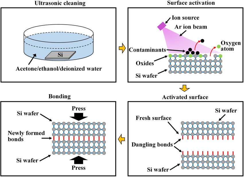
Traditional high-temperature bonding techniques typically require elevated temperatures to achieve fusion and diffusion between different materials. However, such high-temperature processes often introduce issues such as thermal stress, lattice distortion, and the retention of interfacial impurities, all of which can severely impair optical performance and device longevity. In contrast, surface activated bonding is a technique that enables direct bonding between materials at low or room temperature.
The core principle ofsurface activated bonding is to pre-treat the surfaces of the materials—such as by ion bombardment, plasma cleaning, or chemical activation—to effectively remove contaminants, oxide layers, and polishing residues. This treatment also introduces active sites or unsaturated bonds on the surfaces. Once the Er,Yb-doped glass and the Co:spinel crystal have undergone this activation process, they are brought into contact under controlled pressure at a low temperature. At the interface, atomic diffusion and rearrangement occur, leading to the formation of strong covalent bonds. The result is a robust, clean, and high-quality inorganic bond that preserves the intrinsic properties of the materials.
Material Advantages of Er,Yb:Glass and Co:spinel
Er,Yb:Glass, which is glass doped with erbium (Er) and ytterbium (Yb), offers outstanding optical gain and efficient energy transfer properties. Yb ions, with their wide absorption bands, can efficiently capture pump light energy and transfer it to Er ions. Under the right conditions, the excited Er ions then emit laser light—making Er,Yb:Glass particularly well suited for generating eye-safe laser output at the 1.55 μm wavelength.
On the other hand, Co:spinel crystals possess unique magnetic-optical, electrical, and mechanical properties. They are widely used in passive Q-switching and other optical modulation applications. Their inherent mechanical stability, low thermal expansion coefficient, and excellent thermal conductivity make them ideal candidates for reducing thermal distortions in high-power laser systems. By bonding Er,Yb:Glass with Co:spinel using surface activated bonding, the resulting composite not only leverages the superior gain and energy transfer efficiency of the glass but also exploits the advantageous passive Q-switching and thermal management properties of the spinel crystal.
Significant Advantages of Surface Activated Bonding
CryLink’s product page provides a detailed description of the advantages achieved by using surface activated bonding technology for fabricating Er,Yb:Glass + Co:spinel bonding crystals. These advantages include:
- Low-Temperature Processing and Reduced Thermal Stress
Since surface activated bonding occurs at low or ambient temperatures, it avoids the thermal stresses that are typically associated with high-temperature fusion processes. This low-temperature approach ensures that the resulting bonded crystal has minimal internal stress, thereby preserving its optical properties and minimizing losses due to thermal effects. - Pristine Interface and Extremely Low Absorption Loss
Through rigorous pre-treatment, the bonding process removes surface contaminants and oxide layers, resulting in a remarkably clean interface. Studies show that the absorption loss at the bonding interface can be maintained below 20 parts per million (ppm), and the change in the bonding surface profile is minimal (less than λ/8). This level of interface quality is crucial for high-performance laser applications where low optical loss and high transmission efficiency are essential. - Strong Process Control and Broad Applicability
Techniques such as ion bombardment or plasma cleaning allow for fine control over the activation parameters, ensuring precise matching between dissimilar materials. Whether bonding glass to crystal, metal to semiconductor, or constructing complex multilayer structures, the surface activated bonding process operates over a wide process window with excellent repeatability and reliability. - Enhanced Device Performance and Extended Lifespan
The high-quality bond produced by this method maintains the excellent gain characteristics of Er,Yb:Glass and the passive Q-switching functionality of Co:spinel. By reducing thermal gradients and mitigating the thermal lens effect during laser pumping, the bonded crystal exhibits improved beam quality and stability. This, in turn, results in a more stable laser output and a longer operational lifespan—key factors for high-power laser systems.
Applications and Future Prospects
The Er,Yb:Glass + Co:spinel bonding crystals, manufactured using surface activated bonding, significantly improve the energy conversion efficiency and thermal management of laser systems. They are particularly promising for applications in laser ranging, LiDAR (Light Detection and Ranging), optical communication, and medical diagnostics. For instance, in the realm of eye-safe lasers, the 1.55 μm wavelength meets international safety standards and is ideal for long-distance, high-precision measurements even in harsh environmental conditions.
Furthermore, the low-temperature bonding process facilitates the miniaturization and integration of laser components. This opens up opportunities for the development of compact, high-performance laser systems that can be used in autonomous driving, defense, and advanced medical instruments.
Looking ahead, continued research in surface activated bonding is expected to further reduce optical losses and improve bond strength through refined interface engineering. The introduction of new active materials and novel bonding techniques may expand the range of material combinations that can be integrated using this process. As these advancements unfold, the technology will not only drive improvements in laser performance but also pave the way for breakthroughs in quantum sensing, next-generation communication networks, and space exploration applications.
Conclusion
CryLink’s use of surface activated bonding technology represents a significant advancement over traditional high-temperature bonding methods. By enabling the direct bonding of Er,Yb:Glass and Co:spinel crystals at low temperatures, this technique maintains the intrinsic optical and thermal properties of both materials while greatly reducing interface contamination and thermal stress. The result is a high-quality, low-loss, and durable bonded crystal that plays a critical role in high-power, eye-safe laser systems.
The advantages of this technology—low-temperature processing, pristine interface quality, strong process controllability, and enhanced device performance—make Er,Yb:Glass + Co:spinel bonding crystals an indispensable component in modern laser applications. As the demand for high-precision, energy-efficient lasers continues to grow, innovations in surface activated bonding will be key to achieving next-generation laser systems with improved stability, miniaturization, and integrated functionality.
In summary, the CryLink product page demonstrates that the application of surface activated bonding technology to produce Er,Yb:Glass + Co:spinel bonding crystals not only overcomes the limitations of conventional high-temperature processes but also sets a new benchmark for low-loss, high-efficiency laser material integration. With ongoing advancements in materials science and interface engineering, this technology is poised to play an increasingly critical role in the evolution of high-performance laser systems and the broader field of optoelectronics.

Frank
Frank graduated from the University of Shanghai for Science and Technology, majoring in optics. As a technical engineer at Crylink Company, he deeply understands crystal materials and laser components.
Related Video(s) with this Article
Related Product(s) with this Article
Related Application(s) with this Article