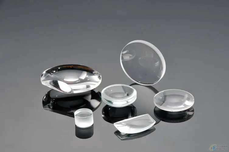
The Pioneering Techniques Behind Membrane Formation
From filtering water to enhancing energy storage capabilities, membranes play a pivotal role in diverse industries. It’s essential to understand the nitty-gritty behind their preparation, as the method chosen can significantly influence a membrane’s final performance. In this comprehensive review, we’ll delve into popular film coating methods that have revolutionized membrane preparation.
Introduction to Membrane Film Coating Techniques
In the world of advanced materials and manufacturing, the importance of membrane film coating techniques cannot be overstated. These methods are fundamental in imparting specific characteristics to surfaces, enhancing their functionality, and ensuring their suitability for varied applications. From the screens we touch to the integrated circuits powering our devices, coatings play a pivotal role. This article delves into three pivotal techniques: physical evaporation, chemical vapor deposition (CVD), and sputtering, shedding light on their processes, advantages, disadvantages, and practical applications.
Physical Evaporation: The Fundamental Process
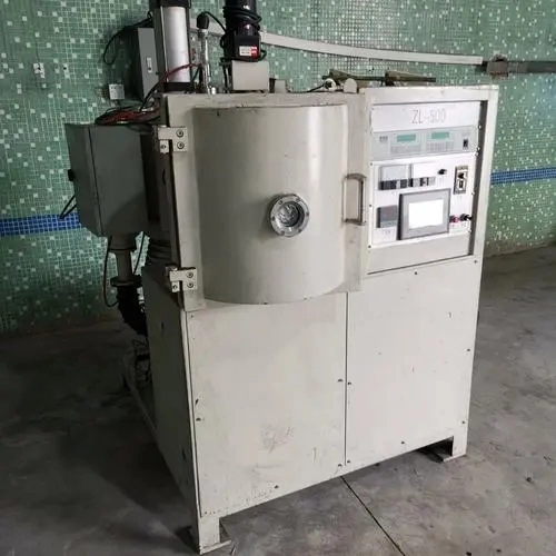
At the heart of physical evaporation lies the principle of transforming materials from a solid to a vapor state. The process involves placing the material in a high vacuum chamber, where it’s heated until it evaporates. As these vaporized particles rise, they meet a cooler substrate where they condense, forming a thin, uniform film.
Advantages: • Simple Process: Fewer components and steps make physical evaporation a straightforward choice for many industries. • Cost-effective: Its simplicity translates to reduced costs, especially for bulk manufacturing.
Disadvantages: • Limited Material Choice: Due to the reliance on high temperatures, not all materials are compatible, limiting its applicability. • Thickness Variability: It often demands skilled technicians to maintain a uniform thickness across the substrate.
Practical Applications: • Beyond optical coatings and mirrors, physical evaporation finds its use in creating metallic films in certain electronic components.
Chemical Vapor Deposition (CVD): Where Chemistry Meets Vapor
Chemical Vapor Deposition offers a marriage between chemical reactions and vapor deposition techniques. Here, gaseous precursors are introduced into a chamber containing the substrate. As these precursors come into contact with the heated substrate, they undergo chemical reactions, breaking down and leaving behind a film on the substrate’s surface.
Advantages: • Versatility: Its ability to coat uneven and complex surfaces makes CVD a versatile tool in the arsenal of coating techniques. • High Purity & Quality: The deposited films are not only of high purity but also exhibit exceptional adhesion, ensuring longevity.
Disadvantages: • Temperature Dependency: While CVD offers many benefits, its reliance on high temperatures makes it unsuitable for substrates that might degrade under heat. • Safety Concerns: Given that some precursors can be toxic or even explosive, there’s a heightened emphasis on safety protocols and handling procedures.
Practical Applications: • CVD isn’t limited to semiconductor production. It’s instrumental in crafting protective coatings for metal components, producing solar panels, and even developing wear-resistant films for tools.
Sputtering: An Electrically Driven Technique
A lesser-known but equally vital method, sputtering involves ejecting material from a “target” that is then deposited on a substrate. This is achieved by creating a plasma in a chamber, where positively charged ions collide with the target material, leading to the ejection of atoms.
Advantages: • Material Diversity: Sputtering can be used with a wide variety of materials, including metals, alloys, and compounds. • Uniform Coatings: It ensures exceptionally uniform coatings even on complex 3D structures.
Disadvantages: • Rate of Deposition: Compared to other techniques, sputtering might have a slower deposition rate. • Cost: The intricacy of the process can sometimes lead to higher costs.
Practical Applications: • Sputtering is crucial in producing thin-film transistors, magnetic recording media, and certain types of architectural glass.
In wrapping up, while each coating technique has its strengths and limitations, their collective contributions to modern technology are undeniable. As research continues and technology advances, we can expect further refinements, expanding the horizons of what’s achievable with membrane film coatings.
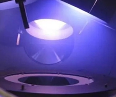
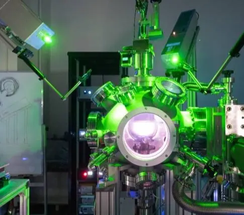
Sputtering: Harnessing the Power of Ions
At the forefront of thin film deposition technologies lies sputtering, a technique that might sound aggressive but is rooted in precision. Imagine a controlled environment, specifically a vacuum chamber, where a target material patiently awaits. When ions, accelerated under an electric field, strike this target, they dislodge its atoms. These ejected atoms, having enough energy, traverse the chamber and gracefully settle onto a substrate. What we get as a result is a meticulously formed thin film.
This process is not merely a collision of particles; it’s an intricate dance of physics, ensuring that materials find a new home on substrates, often in ways that conventional methods can’t replicate.
Advantages:
•Material Diversity: The beauty of sputtering lies in its versatility. Whether it’s metals, insulators, or compounds, almost any material can be sputtered. This opens the doors for experimentation and tailoring the thin films to specific requirements.
•Uniform Coatings: Another feather in sputtering’s cap is the uniformity it brings. The resultant films are not just even across surfaces, but they also exhibit exceptional adhesion, ensuring that the coatings are durable and serve their purpose effectively.
Disadvantages:
•Rate Limitation: While sputtering offers precision, it often does so at a leisurely pace. The deposition rates for sputtering are generally slower compared to some other techniques, which might not be ideal for large-scale or rapid production needs.
•Complexity: Precision often demands sophistication. Sputtering requires intricate machinery and a more elaborate setup. This not only means higher initial investments but also demands skilled technicians to operate and maintain the equipment.
Practical Applications: • The real testament to sputtering’s prowess is its widespread adoption across industries. It’s a darling in the electronics sector, predominantly for crafting thin-film transistors that power our displays. Furthermore, sputtering is pivotal in fabricating sensors that are becoming the backbone of the emerging Internet of Things (IoT) landscape. Additionally, when it comes to safeguarding materials against the ravages of time and environment, sputtering steps in to produce corrosion-resistant coatings that extend the lifespan of various products.
Navigating the Best Fit for Membrane Preparation
In the vast realm of membrane fabrication, understanding and aligning the technique with the end application is an art. The landscape of coating methods is as diverse as the materials and applications they cater to. While the precision and uniformity of sputtering make it a go-to for many electronic applications, the high-purity and chemical versatility of CVD cater to specialized needs, especially when unique material properties are at the forefront. But how does one chart a course through this maze of options?
Factors Influencing Choice
Membrane preparation isn’t a one-size-fits-all affair. Delving deeper, we realize there’s a matrix of considerations to ponder upon:
• Desired Film Properties: Every application has its unique demands. Whether it’s the film’s thickness, its adhesive strength, or its purity level, defining these parameters can significantly narrow down the coating choices.
• Substrate Characteristics: The nature of the substrate is a defining pivot. Fragile or temperature-sensitive substrates may not be compatible with methods that employ high heat, necessitating a more delicate approach.
• Cost Implications: In an industrial setting, the budget often dictates the rhythm. While certain methods might offer unparalleled results, they might also come with a hefty price tag. Striking a balance between cost and quality is crucial.
• Safety: A paramount concern, especially when dealing with volatile chemicals or high temperatures, is safety. The CVD process, with its use of precursor chemicals, is a case in point. Evaluating the safety profile, ensuring proper handling and storage, and complying with regulations are integral components of the decision matrix.
In summary, the journey of membrane preparation is a dance between material science, economics, and safety. With a clear roadmap, one can navigate this intricate path to derive optimal outcomes.
Conclusion
In the realm of membrane preparation, the method makes the membrane. By understanding the intricacies of physical evaporation, chemical vapor deposition, and sputtering, one can craft membranes tailor-made for specific applications. As technology and industry demands evolve, it’s vital to stay abreast of these foundational techniques that underpin the membrane revolution.
FAQs
- 1. Why is uniform thickness crucial in membranes? Uniformity ensures consistent performance and reduces vulnerabilities in the membrane structure.
- 2. Are there hybrid techniques combining these methods? Yes, some processes integrate features from multiple methods to achieve specific deposition outcomes.
- 3. How do we choose between CVD and sputtering for electronic applications? Consider factors like the desired film property, substrate type, budget, and safety implications of precursor materials.
- 4. What role does the substrate play in membrane preparation? The substrate can influence film adherence, quality, and even the choice of deposition method.
- 5. Are these methods suitable for large-scale industrial production? Absolutely. Many of these techniques, especially CVD and sputtering, are scalable and used extensively in industries.

Frank
Frank graduated from the University of Shanghai for Science and Technology, majoring in optics. As a technical engineer at Crylink Company, he deeply understands crystal materials and laser components.
Related Video(s) with this Article
Related Product(s) with this Article
Related Application(s) with this Article