Introduction
In recent years, the applications of Ultraviolet (UV) solid-state lasers have taken a profound leap, transcending from conventional uses to more precision-driven fields. Whether it’s semiconductor processing, intricate micromachining, or the nuances of DNA sequencing, UV lasers’ precise nature is at the forefront of cutting-edge innovations. This article delves deep into the world of UV lasers, outlining their pivotal role in modern-day applications and the crystals that drive these high-performance devices.
The Rise of Ultraviolet Solid-State Laser
Ultraviolet lasers, often hailed as the pinnacle of modern photonics, operate in the unique realm of the electromagnetic spectrum defined by wavelengths between 100 to 400 nanometers. This specific range, invisible to the human eye, offers a myriad of advantages that are not achievable with visible light lasers.
When we talk about the distinct features of UV laser, their ability to produce high-intensity beams stands out. High intensity, in this context, means that the light emitted by these lasers carries a considerable amount of energy per photon. This high energy translates into the capability to interact with a material at the atomic or molecular level, making it an invaluable tool for precision-driven applications. For example, in industries where thin layers of a substance need to be removed without affecting the underlying material, such as in semiconductor manufacturing or in detailed artwork on glass, UV lasers are the tool of choice.
Another pivotal characteristic is the reduced heat associated with UV laser. In many laser applications, heat generation is a significant concern as it can lead to material warping or degradation, especially when working with delicate or thermally sensitive materials. UV lasers, with their minimal heat output, ensure that the surrounding material remains largely unaffected. This damage-free operation is crucial in medical procedures, micromachining, and other areas where the integrity of the surrounding material is paramount.
Moreover, the precision and consistency of UV lasers are unrivaled. They can be tuned to specific frequencies, ensuring that the beam interacts only with selected materials while leaving others untouched. This selective interaction is a boon for researchers and industries that require a high degree of specificity in their operations.
In essence, the rise of ultraviolet solid-state lasers can be attributed to their unique properties that cater to a broad spectrum of applications. From medical surgeries to art restoration and semiconductor fabrication, these lasers have carved a niche for themselves, redefining the boundaries of what’s possible in the world of precision application.
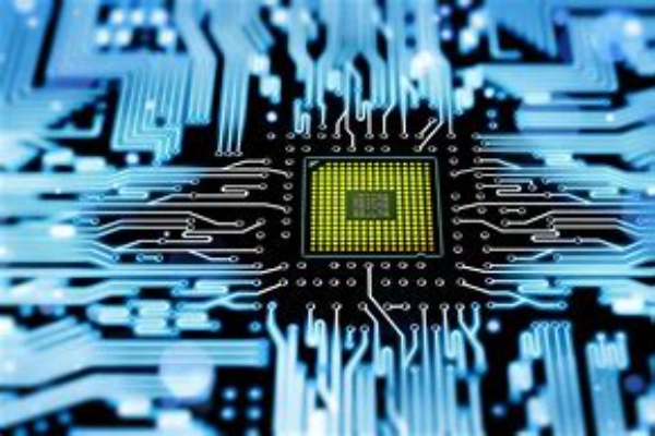
UV Lasers in Semiconductor Processin
Semiconductor processing, the linchpin of our rapidly advancing digital era, demands nothing short of absolute precision. Here, ultraviolet (UV) lasers prove themselves not as mere instruments, but as essential catalysts, driving innovation and accuracy to unprecedented levels.
One of the most critical processes in the semiconductor industry is photolithography, a sophisticated technique responsible for transcribing minute and intricate circuits onto semiconductor wafers. Think of photolithography as the brushstrokes of a masterful artist, where every stroke, every delineation, matters. In this delicate process, UV lasers shine brilliantly. They bring about unparalleled precision, enabling the creation of extremely detailed patterns on semiconductor materials. With each pulse, UV lasers etch the foundation of what eventually becomes the integrated circuits that power our computers, smartphones, and countless other devices.
Simultaneously, the role of UV lasers doesn’t halt at photolithography. They further stretch their potential in processes like doping and annealing. Doping, a procedure where impurities are intentionally introduced into semiconductors to modify their properties, is an art of balance. Too much or too little, or even a slight deviation from the desired location, can compromise the functionality of the semiconductor. UV lasers, with their impeccable accuracy and ability to channel energy meticulously, ensure that the doping process is conducted flawlessly.
Their beams can pinpoint exact locations on the semiconductor wafer, introducing the right amount of impurities without any collateral damage to surrounding areas. Such precision guarantees that the resultant semiconductor not only performs optimally but also remains reliable in the long run.
In essence, as the semiconductor industry continues its relentless pursuit of miniaturization and perfection, UV lasers stand as stalwart allies. Their unparalleled precision and versatility are shaping the very future of technology, ensuring that the digital marvels we rely on become faster, smaller, and more efficient with each passing day.
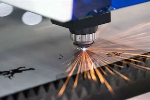
Micromachining Wonders with UV Lasers
In the age of relentless technological progress, the march towards miniaturization is inexorable. As gadgets shrink, so does the demand for smaller, yet more powerful components. Here, ultraviolet (UV) laser emerge as the unsung heroes, standing at the confluence of innovation and precision, reshaping the world of micromachining.
Micromachining is the art and science of fabricating minuscule components, often requiring manipulations at the micrometer or even nanometer scale. UV laser, with their innate ability to produce high-intensity beams, are masters in this domain. Imagine the challenge of cutting or drilling into materials like metals and ceramics without causing undue stress or deformation.
It’s akin to performing a delicate surgery, where every incision must be precise. UV lasers, with their pinpoint accuracy, tackle such tasks with aplomb. Their beams, focused and consistent, glide through materials, creating cuts and holes that are not just accurate but also incredibly smooth. Such finesse is particularly crucial when the components being crafted are destined for high-performance applications like aerospace or medical devices.
Beyond the realms of cutting and drilling, UV lasers continue to weave their magic in surface structuring. Many modern components, whether for aerospace, optics, or electronics, require surfaces with intricate patterns or structures. These could be for enhancing light reflection, ensuring better adhesion, or a myriad of other functional reasons. UV lasers rise to this challenge effortlessly. They dance over surfaces, etching, modifying, and sculpting at microscopic levels. This capability to fine-tune surfaces down to minute details ensures that components not only meet but often exceed performance expectations.
To sum it up, in the intricate ballet of micromachining, UV lasers play the lead role. Their unmatched precision and versatility enable industries to push boundaries, crafting components that are not just smaller, but also significantly superior in performance. As we stand on the brink of more technological revolutions, the prowess of UV lasers in micromachining assures that the future is not just miniature, but also magnificent.
UV Lasers in DNA Sequencin
In the intricate tapestry of genetics, where every thread represents a sequence and every sequence holds the key to life’s mysteries, UV lasers have emerged as invaluable tools. This realm, where precision is paramount and even a minuscule error can skew results, demands the best of technology. And UV lasers, with their unparalleled accuracy, have proven themselves worthy of this monumental task.
Fluorescence detection in DNA sequencing is a testament to the prowess of UV lasers. By stimulating fluorescent markers bound to specific DNA fragments, these lasers illuminate the genetic code, enabling scientists to decipher it. Each pulse of the UV laser evokes a glow from the markers, which in turn translates into a readable sequence. This dance of light and genetics unfolds with such precision that it allows researchers to read vast stretches of DNA with minimal errors, unlocking insights that were once considered unattainable.
Moreover, the exploration doesn’t stop at reading the sequences. UV lasers also play a pivotal role in fragment analysis, another cornerstone of genetic research. By inducing clean and precise breaks in DNA chains, these lasers empower scientists to study fragments individually. Such detailed analysis unravels the nuances of our genetic makeup, paving the way for not just a deeper understanding of genetics, but also breakthroughs in diagnostics and therapeutic interventions.
In essence, UV laser, with their precision and efficiency, have become indispensable allies in the world of genetics. Through their beams, they illuminate the path to a future where the mysteries of DNA are no longer enigmatic but are tools to harness for the betterment of humanity.

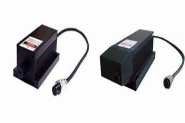
Crystals Powering UV Lasers
Within the heart of every UV laser, crystals stand as the silent custodians of performance, shaping the laser’s efficiency, stability, and precision. The caliber of these crystals can mean the difference between a UV laser that’s merely functional and one that’s exemplary.
Among the luminaries in this realm is the frequency-tripled Nd:YAG crystal. Revered for its stellar attributes, this crystal has entrenched itself as a mainstay in numerous UV laser configurations. The strength of Nd:YAG lies in its inherent ability for third-harmonic generation, a property that allows it to efficiently convert infrared radiation into the ultraviolet spectrum. This seamless conversion ensures that UV lasers equipped with Nd:YAG deliver beams of impeccable consistency, while also boasting a longevity that many other crystals might struggle to match.
However, as technology advances, newer champions are rising to the fore, and Ce:LiCAF stands as a testament to this evolution. Cerium-doped Lithium Calcium Aluminum Fluoride, or Ce:LiCAF for short, is a modern gem in the world of UV lasers. Renowned for its high UV output, this crystal’s stability is a marvel in itself. As industries increasingly seek UV lasers that can operate at peak performance without frequent recalibrations or maintenance, Ce:LiCAF is swiftly emerging as the crystal of choice. Its ability to deliver sustained high-intensity UV beams makes it an invaluable asset for applications demanding the very best.
In summation, while UV lasers are undeniably the marvels of modern photonics, it’s the crystals within that truly define their prowess. From the tried-and-tested Nd:YAG to the promising vistas opened by Ce:LiCAF, these crystals are the unsung heroes, powering the next generation of UV laser systems.
Conclusion
The integration of Ultraviolet solid-state laser in sectors demanding precision underscores their unmatched capabilities. Whether it’s shaping the future of semiconductors, crafting minuscule machine parts, or unravelling the mysteries of human DNA, UV lasers are truly illuminating the path. As technology continues to evolve, their role is only set to become more pivotal, driving innovations and breakthroughs in diverse fields.
FAQs
- What spectrum range do UV lasers typically operate in?
UV lasers usually function within the spectrum of 100 to 400 nanometers. - Why are UV lasers preferred in semiconductor processing?
Their ability to deliver high-intensity beams with minimal heat ensures precise and damage-free operations, crucial for semiconductor processing. - What role do UV lasers play in DNA sequencing?
UV lasers are instrumental in fluorescence detection and fragment analysis, enabling precise genetic research and diagnostics. - Why is the Ce:LiCAF crystal gaining popularity in UV laser systems?
Due to its high UV output, stability, and consistent performance, Ce:LiCAF is becoming a preferred choice for many UV laser applications. - How do UV lasers contribute to micromachining?
UV lasers are ideal for precision cutting, drilling, and surface structuring, especially for miniaturized components.

Frank
Frank graduated from the University of Shanghai for Science and Technology, majoring in optics. As a technical engineer at Crylink Company, he deeply understands crystal materials and laser components.
Related Video(s) with this Article
Related Product(s) with this Article
Related Application(s) with this Article